- 您现在的位置:买卖IC网 > Sheet目录3873 > PIC18F13K50-I/P (Microchip Technology)IC PIC MCU FLASH 4KX16 20-PDIP
2006 Microchip Technology Inc.
Preliminary
DS70178C-page 207
dsPIC30F1010/202X
18.4
PRIMARY OSCILLATOR ON OSC1/
OSC2 PINS:
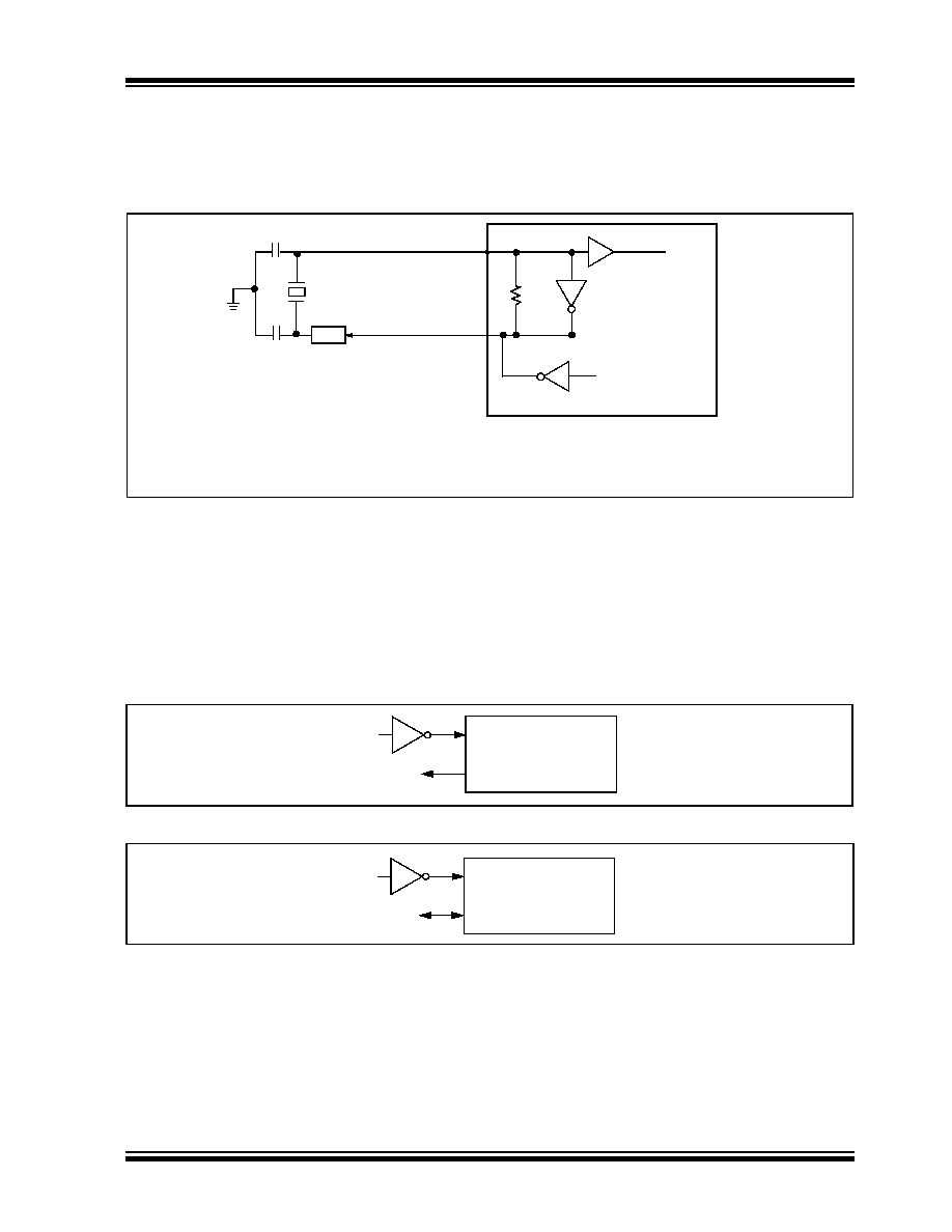
The primary oscillator uses is shown in Figure 18-3.
FIGURE 18-3:
PRIMARY OSCILLATOR
18.5
EXTERNAL CLOCK INPUT
Two of the primary Oscillator modes use an external
clock. These modes are EC and EC with IO.
In the EC mode (Figure 18-4), the OSC1 pin can be
driven by CMOS drivers. In this mode, the OSC1 pin is
high-impedance and the OSC2 pin is the clock output
(FOSC/2). This output clock is useful for testing or
synchronization purposes.
In the EC with IO mode (Figure 18-5), the OSC1 pin
can be driven by CMOS drivers. In this mode, the
OSC1 pin is high-impedance and the OSC2 pin
becomes a general purpose I/O pin. The feedback
device between OSC1 and OSC2 is turned off to save
current.
FIGURE 18-4:
EXTERNAL CLOCK INPUT OPERATION (EC OSCILLATOR CONFIGURATION)
FIGURE 18-5:
EXTERNAL CLOCK INPUT OPERATION (ECIO OSCILLATOR CONFIGURATION)
C1
C2
XTAL
OSC2/CLKO
Rs (1)
OSC1/CLKI
RF (2)
Note 1: A series resistor, Rs, may be required for AT strip cut crystals.
2: The feedback resistor, RF, is typically in the range of 2 to 10 M
Ω.
To CLKGEN
CLKO/RC15
OSC1
OSC2
FOSC/2
dsPIC30F
Clock from Ext System
OSC1
I/O (OSC2)
I/O
dsPIC30F
Clock from Ext System
发布紧急采购,3分钟左右您将得到回复。
相关PDF资料
PIC16CR76T-I/SO
IC PIC MCU 8KX14 28SOIC
PIC18LF24K22-I/MV
IC PIC MCU 16KB FLASH 28UQFN
PIC18LF24K22-I/ML
IC PIC MCU 16KB FLASH 28QFN
PIC16CR76T-I/ML
IC PIC MCU 8KX14 28QFN
PIC16F627-04/P
IC MCU FLASH 1KX14 COMP 18DIP
PIC18F45J10-I/ML
IC PIC MCU FLASH 16KX16 44QFN
PIC18F24K22-I/ML
IC PIC MCU 16KB FLASH 28QFN
PIC16CR76-I/SS
IC PIC MCU 8KX14 28SSOP
相关代理商/技术参数
PIC18F13K50-I/P
制造商:Microchip Technology Inc 功能描述:20 Pin 8 KB Flash 512 RAM 15 I/O 10
PIC18F13K50-I/SO
功能描述:8位微控制器 -MCU 8KB Flash 512 RAM 15 I/O 10-B ADC USB 2.0 RoHS:否 制造商:Silicon Labs 核心:8051 处理器系列:C8051F39x 数据总线宽度:8 bit 最大时钟频率:50 MHz 程序存储器大小:16 KB 数据 RAM 大小:1 KB 片上 ADC:Yes 工作电源电压:1.8 V to 3.6 V 工作温度范围:- 40 C to + 105 C 封装 / 箱体:QFN-20 安装风格:SMD/SMT
PIC18F13K50-I/SO
制造商:Microchip Technology Inc 功能描述:20 Pin 8 KB Flash 512 RAM 15 I/O 10
PIC18F13K50-I/SS
功能描述:8位微控制器 -MCU 8KB Flash 512 RAM 15 I/O 10-B ADC USB 2.0 RoHS:否 制造商:Silicon Labs 核心:8051 处理器系列:C8051F39x 数据总线宽度:8 bit 最大时钟频率:50 MHz 程序存储器大小:16 KB 数据 RAM 大小:1 KB 片上 ADC:Yes 工作电源电压:1.8 V to 3.6 V 工作温度范围:- 40 C to + 105 C 封装 / 箱体:QFN-20 安装风格:SMD/SMT
PIC18F13K50-I/SS
制造商:Microchip Technology Inc 功能描述:8-Bit Microcontroller IC
PIC18F13K50T-I/SO
功能描述:8位微控制器 -MCU 8KB Flash 512 RAM 15 I/O 10-B ADC USB 2.0 RoHS:否 制造商:Silicon Labs 核心:8051 处理器系列:C8051F39x 数据总线宽度:8 bit 最大时钟频率:50 MHz 程序存储器大小:16 KB 数据 RAM 大小:1 KB 片上 ADC:Yes 工作电源电压:1.8 V to 3.6 V 工作温度范围:- 40 C to + 105 C 封装 / 箱体:QFN-20 安装风格:SMD/SMT
PIC18F13K50T-I/SS
功能描述:8位微控制器 -MCU 8KB Flash 512 RAM 15 I/O 10-B ADC USB 2.0 RoHS:否 制造商:Silicon Labs 核心:8051 处理器系列:C8051F39x 数据总线宽度:8 bit 最大时钟频率:50 MHz 程序存储器大小:16 KB 数据 RAM 大小:1 KB 片上 ADC:Yes 工作电源电压:1.8 V to 3.6 V 工作温度范围:- 40 C to + 105 C 封装 / 箱体:QFN-20 安装风格:SMD/SMT
PIC18F14K22-E/ML
功能描述:8位微控制器 -MCU 16KBFlash 512byteRAM 256bytesEEPROM
RoHS:否 制造商:Silicon Labs 核心:8051 处理器系列:C8051F39x 数据总线宽度:8 bit 最大时钟频率:50 MHz 程序存储器大小:16 KB 数据 RAM 大小:1 KB 片上 ADC:Yes 工作电源电压:1.8 V to 3.6 V 工作温度范围:- 40 C to + 105 C 封装 / 箱体:QFN-20 安装风格:SMD/SMT